Solutions » Introduction to Industry-Specific Solutions » Photovoltaic Cell Manufacturing Process Equipment »
CVD

- Energy Saving


- By Industry ⁄ Process


- Applications


|CVD
4p-i-n Layer Formation
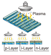
Plasma is applied to form each layer.